TL;DR
- Switch 2 features Nvidia T239 SoC with 8x Arm Cortex-A78 CPU cores and Ampere-based GPU
- Performance reaches 7.5x original Switch with docked mode matching GTX 1050 Ti performance
- 12GB LPDDR5X RAM and 256GB UFS 3.1 storage provide significant upgrades
- Power consumption peaks at 34.4W with advanced cooling requirements for sustained performance
- Real-time ray tracing and DLSS support enable next-generation gaming experiences
While Nintendo officially revealed the Switch 2 console recently, detailed technical specifications remained scarce until Chinese tech channel Geekerwan conducted an extensive reverse-engineering analysis of the device’s motherboard. Their investigation provides unprecedented insights into the hardware architecture, performance capabilities, and gaming potential of Nintendo’s next-generation handheld console.
This comprehensive examination reveals critical details about the Switch 2’s processing capabilities, memory architecture, and thermal design considerations that will impact gaming performance and user experience.
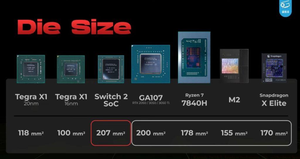
Geekerwan’s investigation confirms the Nintendo Switch 2 is powered by Nvidia’s custom T239 system-on-chip, which completed initial development in 2021. Through sophisticated Focused Ion Beam Scanning Electron Microscopy (FIB-SEM) analysis, researchers determined the chip likely utilizes Samsung’s hybrid 10nm/8nm fabrication process, which Nvidia markets as their proprietary “8N” manufacturing node.
The T239 SoC features a substantial die size measuring approximately 207 square millimeters, representing roughly double the surface area of the Tegra X1 chip found in the original Switch. This expanded physical footprint places it in similar territory to discrete GPUs like the RTX 3050 and 2050, while exceeding the die sizes of modern processors including Ryzen 7 7840H, Apple M2, and Snapdragon X Elite platforms.
Power consumption analysis reveals the T239 chip can reach peak power draw of 34.4 watts under maximum load conditions. While this represents significant thermal output for a handheld device, actual gaming usage will likely maintain lower power levels to balance performance with battery life considerations.
The Nvidia T239 chipset incorporates what appears to be an Ampere-based graphics processing unit architecture featuring six Texture Processing Clusters (TPCs). This configuration delivers twelve Streaming Multiprocessors (SMs) totaling 1,536 CUDA cores for parallel processing capabilities. Current information doesn’t confirm the presence of dedicated ray tracing units or Tensor cores for AI acceleration.
GPU clock speeds demonstrate significant variance between operational modes, with handheld mode reaching up to 561MHz while docked configuration enables frequencies up to 1007MHz. To estimate real-world graphics performance, Geekerwan conducted innovative testing by downclocking an RTX 2050 laptop GPU to simulate the Switch 2’s expected performance profile.
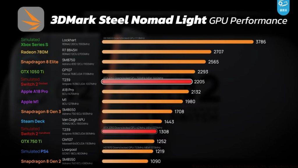
The performance simulation methodology provides valuable insights into how the Switch 2 will handle modern gaming workloads, though actual performance may vary based on final optimization and driver implementation.
In comprehensive 3DMark Steel Nomad Light benchmark testing, the simulated Switch 2 GPU achieved scores of 2,205 points in docked mode and 1,308 points during handheld operation. These results position the console’s graphics performance approximately equivalent to a desktop GTX 1050 Ti when docked, while handheld performance exceeds the GTX 750 Ti but falls slightly below Valve’s Steam Deck capabilities.
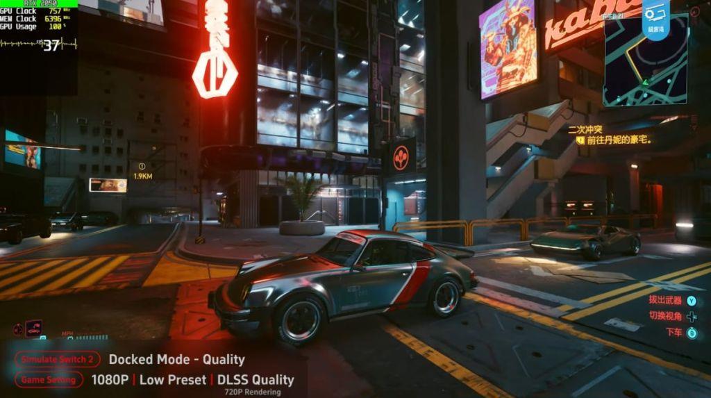
Real-world gaming tests demonstrate the Switch 2’s ability to handle demanding titles like Cyberpunk 2077 with appropriate settings adjustments. The inclusion of real-time ray tracing and DLSS support suggests Nintendo aims to deliver next-generation visual features previously unavailable on handheld platforms.
Performance optimization strategies will be crucial for developers seeking to maximize the hardware’s potential while maintaining acceptable battery life during portable gaming sessions.
| Specs | Nintendo Switch 2 (Leaked) |
|---|---|
| Fabrication | Samsung’s 10nm/8nm hybrid (likely) |
| SoC | Nvidia T239 Chip |
| CPU | 8x Arm Cortex-A78 cores Up to 1.1GHz (Handheld) Up to 1.0GHz (Docked) |
| GPU | Ampere-based Nvidia GPU (likely) 6 TPCs, 12 SMs, 1536 CUDA cores Up to 561MHz (Handheld) Up to 1007MHz (Docked) Real-time Ray Tracing and DLSS Support |
| Memory | 2x 6GB LPDDR5X memory from SK hynix Total 12GB RAM 128-bit, Up to 8533MT/s |
| Storage | TLC-based 256GB UFS 3.1 from SK hynix |
| Maximum SoC Power | 34.4W |
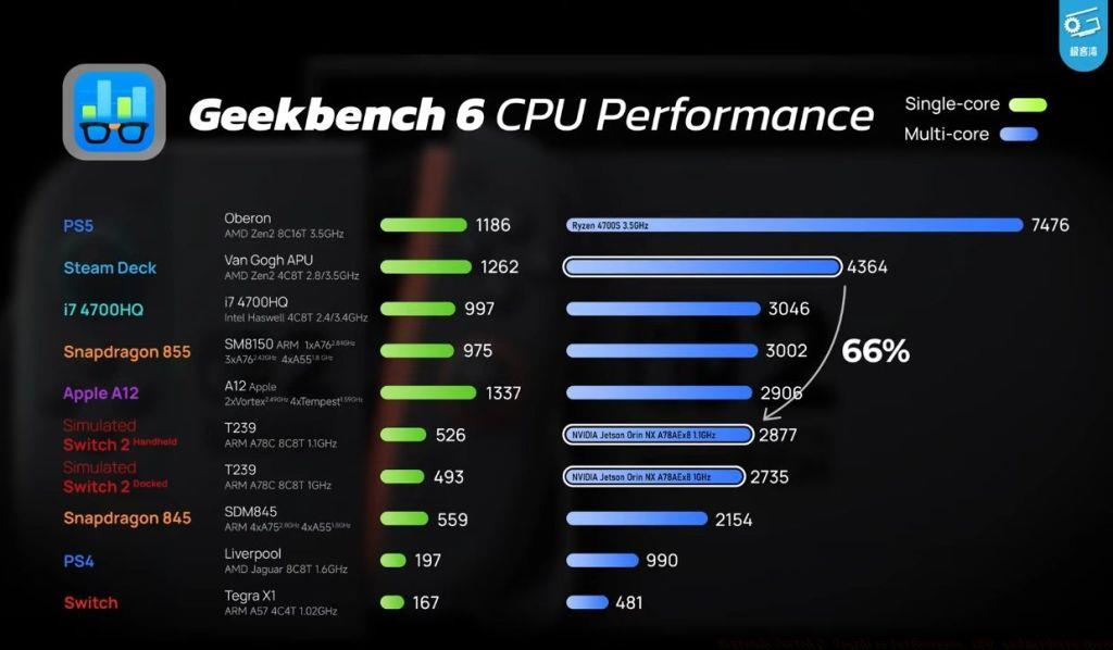
The Switch 2’s processing capabilities are driven by eight Arm Cortex-A78 CPU cores, representing a substantial upgrade over previous generation mobile processors. The CPU operates at frequencies up to 1.1GHz in handheld mode and 1.0GHz when docked, suggesting sophisticated power management strategies.
Memory architecture utilizes two 6GB LPDDR5X modules from SK hynix, delivering a total of 12GB system memory with 128-bit interface operating at speeds up to 8533MT/s. Storage solutions incorporate TLC-based 256GB UFS 3.1 storage, providing significant improvements in loading times and game installation capacity compared to previous Nintendo systems.
Action Checklist
- Monitor thermal performance during extended gaming sessions to identify potential throttling issues
- Adjust graphics settings based on performance mode (handheld vs docked) for optimal experience
- Utilize DLSS technology when available to maximize visual quality while maintaining performance
- Manage storage space efficiently with 256GB capacity for game installations
- Compare performance metrics with competing handheld devices to understand relative capabilities
No reproduction without permission:Tsp Game Club » Nintendo Switch 2: Graphics Performance, CPU, and Hardware Specs Comprehensive analysis of Nintendo Switch 2 hardware specs, performance benchmarks, and gaming capabilities